Empowering Growth with Seamless Technical Solutions

Your Trusted Partner for maximizing Impacts and Results

image-1
Services

Architecture and Design Expertise

We are well established semiconductor design company in India. Digicomm Semiconductor has developed expertise as a young semiconductor solutions provider making it one of the best semiconductors service company around implementing complex algorithmic designs. Our designed semiconductor has made us one of the best semiconductor company in India.

  • uArch Specification to Net list
  • Chip planning, interface details and detailed micro architecture for all PD modules.
  • Experience in leading and implementing complex algorithmic designs.
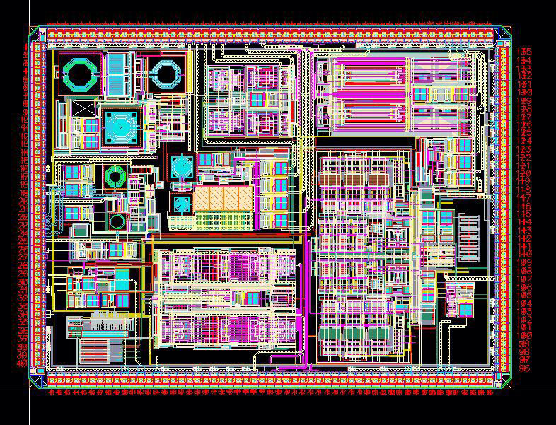
  • Designed chip up to 16FF technology with more than 12M instances and up to 512Mb embedded memory.
  • Experience in designing for timing closure friendly for speed up to 1.2GHz.
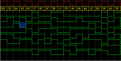
  • Ethernet and Interlaken Phy and MAC designs.
  • PCIe implementation up to Gen4 and 16-lanes supporting 1, 2 or 4 ports
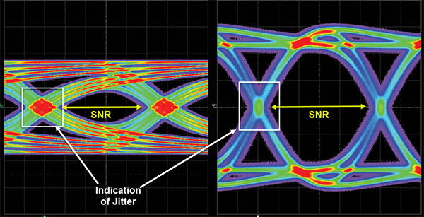
  • Up to 48 56G PAM4 serdes integration.
  • AVS and power islands for power saving.
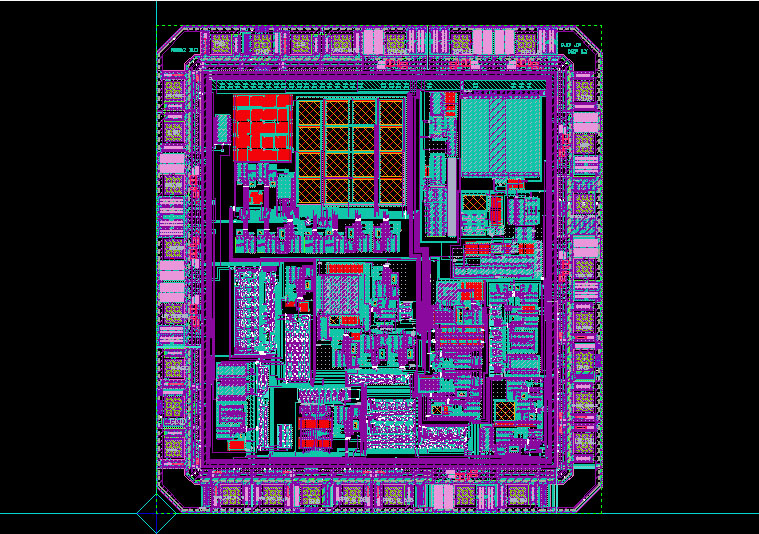
Design Verification Expertise

  • SoC, ASIC Full-chip, Sub-system and IP level Verification
  • VIP/BFMs, Protocol monitors and checkers
  • Mixed-language verification using SystemVerilog, Specman-e, Vera, C/C++, Verilog/VHDL OVM, VMM and UVM based environment
  • DArchitecture models in C / System Verilog
  • Directed & Constrained Random verification
  • Functional coverage driven verification
image-1
  • Code coverage analysis
  • Assertion based formal verification
  • Low Power Design verification
  • Gate Level Simulations
  • Formal Verification
  • Emulations using Palladium
  • Chip bringup and ATE Vector Generation & Support

DFT Expertise

  • uArch Specification to Net list
  • Mentor Tessent/Synopsys DFT compiler for hierarchical scan insertion
  • Option to insert membist in RTL or netlist
  • BISR chain for auto loading all needed redundancy and configuration from OTP/Efuse
  • Experience in designing for timing closure friendly for speed up to 1.2GHz.
  • At-speed scan and LBIST to cover more than 99% of logic
  • Extensive experience in bringing up chip in ATE and support till production including HTOL, ESD, functional validation in the lab.
image-1
image-1

Physical Design Implementation Expertisee

    PD implementation

  • Floor planning
  • Place and Route
  • CTS

    STA & Design Analysis

  • Constraint Generation
  • Budgeting
  • Timing Sign of
  • Timing Sign of
  • Xtalk, Noise ,Signal integrity
  • AOCV and POCV

    Physical Verification & DFM

  • LVS, DRC, EEC, ESD, Antenna
  • OPC, CMP, Yield, etc.

Analog & Mixed Signal Layout Expertise

  • Exposure to multiple technology nodes, TSMC FinFet up to 3nm & GF – FDSOI
  • High speed design in the range of 32/64 Gbps, Power management, Memory, RF, Data Converters and pure analog modules.
  • IP delivery – complete ownership and delivery of IP starting from Transistor level to Bump and ESD planning.
  • Module or block level delivery engagement.
  • EMIR, thermal aware EMIR, DFM, Density, Client specific custom rules and support to PD/chip level issues.
  • Post layout support.
  • Skill automation for productive layouts
image-1